Basics of Plasma
We are all surrounded by matter in its basic three forms i.e., solid, liquid and gases which
human have always been exploiting for their living needs and well being. With increasing energy input, the state of matter changes from solid to liquid to gaseous and if additional energy is then fed into a gas, it will turn into plasma. It is said that more than 99% of the
matter in the universe is in the state of plasma, which can amongst others be found in the sun or stars. Knowing the existence of plasma in the universe as a whole and on the earth in particular for its applications has always been a subject of research interest. Plasma was first discovered by Irving Langmuir in 1928. Plasma can be seen in its natural form on earth as lightning or as polar light in the Arctic and Antarctic, for example. During a solar
eclipse, plasma can be observed as a bright circle of light (corona) around the sun. Plasmas are made up of atoms in which some or all of the electrons have been stripped away and positively charged nuclei, called ions, roam freely. Plasma is a quasineutral (the number of negatively charged electrons equals the number of positively charged protons) gas of charged and neutral particles which exhibits collective behavior with strong Coulomb (or electrostatic) interactions.
Every ionized gas is not taken as plasma and to be called it as plasma, it must satisfy three conditions i.e., i) Debye length (λD) (a measure of the shielding distance or thickness of the sheath) << dimensions of plasma (L), ii) Number of particles in a Debye sphere (ND)>>>1, and iii) collision parameter (ωτ) >1, where ω–frequency of plasma oscillations and τ is the mean time between collisions with neutral atoms. Being made of charged particles, plasmas can do things gases cannot, like conduct electricity. And since moving charges make magnetic fields, plasmas also can have them due to which plasmas behave uniquely and are said to have their own mind. For example, a magnetic field can create a population of very fast particles. Most plasmas aren’t dense enough for particles to collide with one another very often, so the magnetic and electrostatic interactions become more important. Speaking of electrostatic interactions, because particles in plasma – the electrons and ions – can interact via electricity and magnetism, they can do so at far greater distances than an ordinary gas. That in turn means waves become more important when discussing what goes on in plasma. One such wave is called an Alfvén wave, named for Swedish physicist and Nobel laureate (1970) Hannes Alfvén. Another characteristic of plasmas is the possibility of their confinement (to be held in place).
Plasma Energy Changes World
There are many examples where plasma can be seen in action as: fluorescent light bulb or neon sign and plasma televisions. In a plasma TV, a gas – usually argon, neon or xenon – is injected into a sealed gap between two glass panels. An electrical current is passed through the gas, which causes it to glow. The plasma excites red, green and blue phosphors, which combine to give off specific colors. Another use for plasma is in plasma globes, which are full of noble gas mixes that produce the colors of the ‘lightning’ inside them when an electric current ionizes the gas. The term plasma designates matter with a high, unstable energy level, therefore, when plasma comes in contact with solid materials like plastics and metals, its energy acts on the surfaces and changes important properties, such as the surface energy. In the manufacturing industry, this principle is used for selective modification of material characteristics. Treatment with open air plasma energy causes a targeted and exactly adjustable increase in the adhesiveness and wettability of surfaces. This makes it possible to use completely new (even non-polar) materials and environmentally-friendly, solvent-free paints and adhesives industrially. Today, many chemical surface treatment processes are being replaced with open air plasma treatment. The need in industry to optimize every aspect of a product has become necessary to remain competitive and therefore, no industry is untouched by the application of plasma in the area of optimized product performance. Some of the markets that have seen the most growth in application of plasma are: electronics, aerospace, automotive, food packaging, glass, marine, medical, military, optics, packaging, paint, paper, plastics, and textiles. New applications are being developed daily and the field continues to grow at an enormous rate, because it offers an environmentally friendly and cost effective alternative to wet chemistries. It is no exaggeration to mention that in today’s fast paced market the application of plasma is limited only by our own ability to innovate, the need to drive our product market and apply the technology at hand.
Applications in Electronics
The electronics industry is the modern ‘toolmaker’ for the world economy and as such helps to generate jobs and improve productivity in most other industries. Automobiles, airplanes, telephones, dishwashers, and microwave ovens, to name but a few products, all have electronic components. The sophistication of any national defense relies on electronic components to provide missile guidance, antimissile defense, pinpoint bombing accuracy, and range finding, again to name but a few applications. In the electronics industry, plasma pretreatment is a key asset for achieving cost-effectiveness and process reliability. For transparent, scratch-proof coating of displays, it significantly reduces the reject rate and ensures a flawless appearance. Printing electrically conductive coatings on printed circuit boards, prior plasma activation, micro fine cleaning and electrostatic discharge ensure that the coating will adhere securely. Modern touch screens, LCD displays, smart phones and TV screens make high demands on production processes as the plastic parts must be provided with highly transparent scratch-proof and anti-static coatings before they are bonded. The high degree of automation in the electronics industry demands a surface treatment process that can perform in line with the utmost reliability, delivering a high degree of activation at high speed. The micro-fine atmospheric plasma cleaning and plasma activation provided the electronics industry extremely effective solutions. Plastic displays are treated with plasma directly before application of the antistatic and scratchproof coating in the coater. Thanks to the high surface energy achieved by plasma technology, the applied coating spreads evenly to form a homogeneous film. This results in a flawless appearance and significantly reduces reject rates in production. Plasma treatment offers many persuasive advantages to electronic manufacturing and assembly as:
• Suitable for both selective and large-area surface pretreatment
• Higher quality coating and higher quality adhesion with lower error rates
• Outstanding control of physical process compared to wet chemical processes
• Significant simplification of your process chain, and
• Ecologically responsible because it produces no waste products.
From a long list of possible applications of plasma in electronics industry, some of such applications are being summarized as:
Manufacturing with Plasma
In today’s consumer electronics market, design, appearance and feel are primary drivers in purchase decisions, in addition to pure technical functionality. Top quality design of the casing is particularly important for mobile telephones. Along with general quality and design, manufacturers are looking increasingly to environmentally friendly manufacturing technologies and avoiding the use of VOC’s (volatile organic compounds). Silicon wafers, chips, and high-performance semiconductors are highly sensitive electronic components. As these technologies have developed, so has low-pressure plasma technology as a manufacturing process. The enhancement of the plasma process under atmospheric pressure opens up entirely new possibilities, in particular, for automation. A vacuum is no longer required for plasma treatment, so process flows can be greatly simplified. Plasma treatment has been successfully used to achieve quality finishes with following advantages:
-
Plasma energy reliably removes all particles using super-fine cleaning
-
Greater surface tension on the plastic casing significantly improves finish dispersion and adhesion and makes it possible to use water-based finishes
-
The scrap rate in the finishing stage of production is significantly reduced
-
Plasma technology can be integrated inline in existing finishing lines
-
Higher production speeds mean noticeable cost savings
Plasma coating: Affording electronic units and components selective protection against climatic effects is of utmost importance to the reliability of a wide variety of products. Almost half of all defects on modern passenger cars are attributable to climatically induced aging and corrosion damage to electronic components. Protection against humidity, chemicals and harmful gases – even under extreme temperatures – is an essential pre-requisite for avoiding such system failures. These requirements are presently mainly fulfilled by coatings from paint systems, polymer embedding compounds or gels (silicones). Their use, however, is reaching its limits in terms of economy and ecology given that their application is laborious and time-intensive. The usually solvent-based systems can only be applied with comparatively thick coating thicknesses and little selectivity. Depending on the type of protective coating, additional disadvantages may occur such as poor heat dissipation, absorption of moisture, and delamination of the applied overcoat or undesired attenuation of the sensors. The objective is to give electronic components a thin and long-time stable, selective anti-corrosion coating as a protection against corrosive influences and extreme climatic conditions, and all this in an economical and resource-efficient manner. The deposition of these coatings is accomplished by means of the process providing for plasma polymerization at atmospheric pressure. Companies have succeeded in the development of a new coating process for electronic components using the plasma technology. By employing this process it is possible to effectively deposit thin, transparent and insulating plasma-polymer anti-aging coatings and to selectively protect electronic units and especially printed circuit boards. Thanks to the high barrier effect of the thin coatings, not only a longer lifetime and product safety can be achieved but also a significant cost reduction.
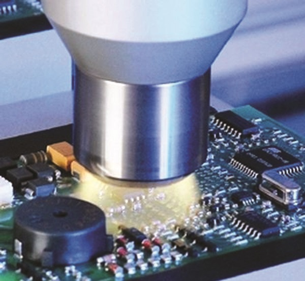
Printed Circuit Boards (PCB): The circuit boards are printed with electrically conductive ink in a screen printing process. Activation with plasma is a prerequisite to ensure safe wetting of the substrate with the conductive ink as well as to achieve good adhesion of the ink to the substrate. Earlier this was executed using low pressure plasma in a vacuum chamber. This method was effective but not suited for the pretreatment of large quantities. The process times used to be too long, and integration into the existing screen printing production lines was not possible. Adding to this was the labor-intensive operation for equipping the vacuum chamber. The rotary nozzle used in this application takes at most one second for the activation of one circuit board panel. The plasma flowing onto the surface at almost ultrasonic speed also removes particles adhering to the surface and neutralizes the electrostatic charge of the circuit board after unpacking. Advantages of Plasma treatment for printed circuit boards:
-
Potential-free surface treatment (e.g., super-fine printed circuit board cleaning)
-
Makes new, more efficient process architectures feasible
-
Eliminates whole production lines in the manufacturing process
-
Makes it possible to selectively activate plasma in electronic components.
Plasma activation: Plasma activation of electronic connectors and sensors prior to potting and encapsulation ensures an excellent hermetic seal, reduces current leakage and provides stronger physical bonding to the device. Plasma activation raises surface energies and ensures good wettability, and more complete flow of resins onto almost all low energy polymer materials. Surface activation of the components’ surfaces and the chips using plasma has shown a significant improvement in the performance of the adhesive used to fix the components in place for further processing in the solder bath. Plasma activation results in an exceptionally effective joining of advanced materials and combinations with a variety of plastics.
Plasma bonding: Polymer surfaces are made bondable by the reactive chemistry present in the plasma. New chemical functional groups are formed with strong chemical bonds to the bulk of the plastic allowing both aqueous based solutions and adhesives to wet into every crevice of the material. This allows a tremendous improvement in bonding, sometimes up to 50 times the strength of the traditional bond.
Plasma cleaning: Clean contact surfaces on the lead frame are essential to ensure reliable contacting of the die with the lead frame. Even the slightest organic contamination reduces the quality of the aluminum-to-copper bonds. It will not be possible to generate enough heat to melt the wire, so the resulting bond will be a cold one. Cleaning of the lead frames before wire-bonding, either by low-pressure plasma removes organic contaminants effectively and reliably.
Moisture impermeability: From high-voltage lines to surface mount components (SMDs), plastic-to-metal bonds are commonly used to fix electrical contacts and protect them against external environmental (weather) conditions. Metal contacts can be made of tinned alloys, aluminum, copper or even gold plating. The area surrounding the plastic-to-metal bond is prone to attack by a wide range of chemicals. Since the metal surface is polar, and has a high affinity for fluids (such as water, grease and oil), a film of moisture often collects on metal contacts. This can lead to corrosion that reduces the adhesion of the chemical bond (except for gold). Plasma treatment provides solutions that reliably and durably prevent creep corrosion around metal contacts. The metal surface is coated with a plasma-deposited nano-scale polymer layer that levels the surface and fills gaps. The polymer coating creates optimal conditions for bonding of the plastic in injection molding and extrusion processes.
Use in LEDs
Light Emitting Diodes (LEDs) technology has developed at a very rapid pace for general-purpose lighting applications with some outstanding advantages in comparison to traditional lighting technologies as extremely long lifetimes, scalable in size, and substantially more energy efficient. Despite these benefits, LEDs also pose several new challenges for the lighting industry. The mechanical design of LED sources will need to be adapted to correct for the more focused and intensive light footprint of LEDs. The LEDs diodes themselves must be effectively protected from environmental influences that can shift the color of the LED, or cause it to fail altogether. New technologies that improve the efficiency and economics of LED production are also needed. Large-format screens comprise many high-powered LEDs. These are potted in a temperature-resistant silicone compound to protect them from environmental factors. While manufacturing displays, the LEDs are mounted on printed circuit boards by the wave-soldering method, the silicone potting compound can pick up residual tin from this bath, which leads to a high reject rate. Using plasma technology has succeeded in depositing an anti-stick, ultrathin layer of glass (SiOx) on the silicone. This layer protects the LEDs during the soldering process. Both atmospheric-pressure and low-pressure plasma technology offer solutions that explicitly meet these LED manufacturing challenges:
-
Lead frame cleaning before the wire-bond process
-
Reduction of copper lead frames
-
Improving adhesion of potting compounds to the molding compound
-
Applying an anti-stick layer on silicone mouldings
Conclusion
In the world of electronics, plasma technology is a critical component on which the industry rests. Though, the primary use of plasmas in the electronics industry is in semiconductor chip manufacturing, however, device dimensions have consistently shrunk with time as technology has incrementally evolved. Besides finer device dimensions, another trend is to make use of stacked layers of materials for interconnection between devices: current devices make use of three levels of metals and insulators, whereas next-generation devices will use four, five, and six levels. These trends place increased demands and increased reliance on plasma processes for high-fidelity pattern transfer, low-temperature deposition, and gaseous cleaning. For example, in the fabrication of the interconnection structure, plasmas are used for deposition of dielectrics and metals, for etching contact windows and conducting patterns, and for cleaning surfaces between each of these steps. Therefore, to produce reliable, cost-effective, environmental-friendly electronic devices for special applications and needs, optimal plasma process of electronic components can play a great role.

If you want to share thoughts or feedback then please leave a comment below.