Energy plays a pivotal role in our daily activities. The degree of development and civilization of a country is measured by the utilisation of energy by human beings. Energy demand is increasing day by day due to increase in population, urbanization and industrialisation. The world’s fossil fuel supply via coal, petroleum and natural gas will thus be depleted in a few hundred years. The rate of energy consumption increasing, supply is depleting in inflation and energy shortage. This is called energy crisis. Hence, alternative or renewable sources of energy have to be developed to meet future energy requirement.
Due to this reason usage of non conventional energy resources such as hydropower, wind is rapidly increasing. Countries having hydro potential are implementing different turbines technologies for generating electricity and to help utility. Similarly, Wind energy sector is also achieving the progress in wind turbines. In addition to this, the most promising source of renewable power today, is photovoltaic system.
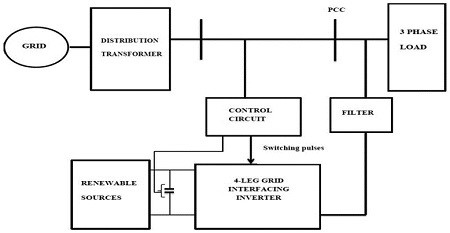
Figure 1: Block diagram…
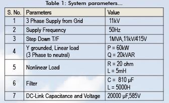
Table 1: System parameters…
Photovoltaic system (PV) as a RES. Output of PV is DC and it needs to be converted to AC before injecting to grid. In order to have satisfactory output; it is of prime importance to develop control schemes for the grid coupled inverters which are used for DC to AC conversion. In this article, we explain the block diagram and simulink model. Carrier based control scheme is mentioned in it. Simulation results and conclusion are also elaborated in detail.
System Model And Assumptions
A. System Configuration
Different blocks for the system under consideration are mentioned in Fig.1. Here we are using 11kV, 50Hz grid. For injecting output of PV at distribution point, we are using 3phase 4 wire transmission network. A voltage source inverter is used for converting DC output of PV system to AC. In addition to this, DC link capacitor is used for having control on 2 sides of the inverter namely; grid side and load side. Control circuit is having logic implemented for carrier based SVPWM. Here, we are analysing the carrier based SVPWM results for both linear as well as non linear load. Lastly, LC filter is also used to minimise harmonics arising due to non linear load switching.
B. Overall Model of the System
By following the above block diagram we have prepared simulink model as shown in Fig. 2. System parameters are mentioned in Table I.
C. Solar Photovoltaic Model
Inverter block shown in above model consists of subsystem of solar panel as well as SVPWM control scheme for inverter. It is as shown in Figure 2.
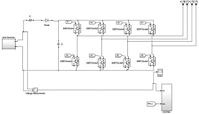
Figure 2: Subsystem of Inverter Block…
Solar panel array is composed of PVA model as shown in Figure 3. Here, Subsystem 1 is representing the model as revealed in Figure 4. In this model, there is subsystem 2 which includes the mathematical model of PV cell.

Figure 3: PVA Model…
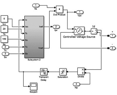
Figure 4: Subsystem 1…
Control Scheme
Grid Synchronisation
Output of inverter must be synchronised with the grid. This can be achieved using Phase Lock Loop (PLL). Unit vector templates derived from data extracted by PLL through grid are stated as in (4), (5) and (6).
Ua = sin θ (4)
Ub = sin (θ – 2Π/3) (5)
Uc = sin (θ + 2Π/3) (6)
Instantaneous values of voltages can be derived using above unit vectors. These are given by (7), (8) and (9).
V*a = Vm x Ua (7)
V*b = Vm x Ub (8)
V*c = Vm x Uc (9)
Where, Vm is the output of PI controller. Error between the reference voltage V*dc and the DC output of PV which are given as inputs for the PI controller generates the active voltage component Vm. Here, we are considering the balanced 3 phase system and thus maintaining neutral current as zero using 4th leg of inverter and hysteresis current controller.
Carrier Based SVPWM
In this article, we have proposed a carrier based SVM whose simulink model is as shown in Figure 5. Modulating signals obtained after grid synchronisation are added to offset voltage. The modified signals are compared with the high frequency triangular carrier to produce gating signals for inverter switches.
Voffset = – (Vmaximum + Vminimum / 2) (10)
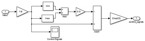
Figure 5: Carrier based SVPWM…
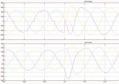
Figure 6: Grid voltage & current…
Simulation Results
Power obtained from photovoltaic system is injected into the grid at t = 0.3 sec. Waveforms for grid, inverter and load are as shown below Fig. 6, 7 & 8. We can clearly observe that after injection of renewable energy via inverter, we are getting smooth sinusoidal output along with the improvement of voltage profile. As PV power drives the load, we can also get the reactive power compensation for load. It is shown in Figure 9.
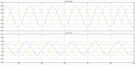
Figure 7: Inverter voltage & current…
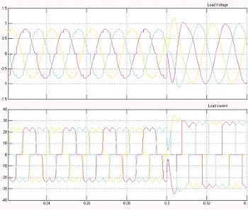
Figure 8: Load voltage & current…
Fast fourier analysis for calculating the parentage of total harmonic distortion is performed which revealed that harmonic distortion gets reduced from 7.38% to 2.45%.Refer Figures 10 & 11.
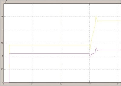
Figure 9: Active and reactive power of load…
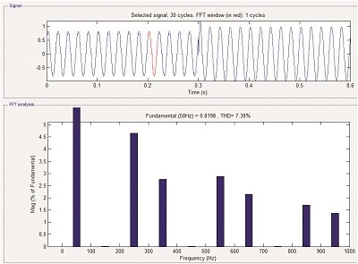
Figure 10: Before injecting PV power…
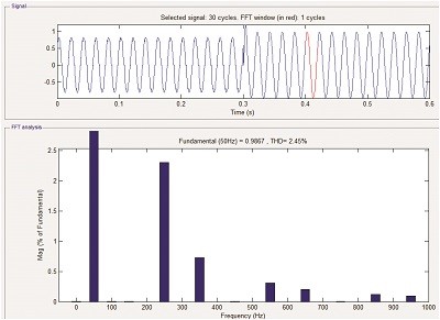
Figure 11: After injecting PV power…
Conclusion
Space vector method used in this project helps in improving voltage profile of the system. Also, we can compensate for reactive power. Total harmonic distortion of the voltage can be reduced to the acceptable value as DC utilisation is maximum in this method. As compare to sine triangle PWM method, this method is very simple in application. We can easily have its implementation for multilevel inverters also.
If you want to share any thoughts or feedback then please leave a comment below.