
In a large EHV Grid system, the circuit breakers are the most important equipment. Failure of any EHV circuit breaker may cause disastrous disturbance in the grid system leading to even grid failure. The failure of circuit breaker may take place due to the transient conditions developed while switching-in and/or switching-out conditions of the circuit breakers used for following equipment or transmission lines.
- Shunt capacitor banks
• Shunt Reactors
• No-Load transformers
• No-Load Overhead transmission lines
• Shunt and series compensated Transmission lines, etc.
Use of “Controlled Switching Device”, an intelligent and smart IED is the only answer to obviate such conditions and to safe guard the circuit breakers against failures due to switching transients.
In this article a basic duty of a “Controlled Switching Device” in back to back switching of a shunt capacitor banks has been explained. The Transients developed are very high in nature and are very injurious to the circuit breaker used for this duty.
A case study, highlighting the need for implementing such device for back to back switching of shunt capacitor banks is also described.
Smart Controlled Switching Device
In order to safeguard the catastrophic failure of EHV circuit breakers and ill-effects on the associated EHV equipment while performing switching-in/off duties particularly in case of back to back switching, a modern smart device named as “Controlled Switching Device“ has been innovated which has an IED (intelligent Electronic Device) through which the programmed command is given for switching-in/off of the circuit breaker contacts at the point “0” position on the voltage wave. This shall safe guard the Circuit Breakers from ill-effects of Switching Transients.

Figure 1: SLD showing Shunt Capacitor banks,C1 & C2 connected to the common EHV Bus
Phenomenon of In-rush transients in Back to Back Switching
The figure 1 shows the basic schematic single line diagram of a power system feeding EHV bus, on which Capacitor banks C1 & C2, each having individual circuit breakers, CB1 & CB 2 are connected through bus-section circuit breaker BSCB.
While Capacitor bank C1 is already connected to the energized EHV bus, the second capacitor bank C2 is now switched-on to the same bus in parallel to the existing Shunt capacitor bank C1. The inrush high frequency transient Currents shall rush to the 2nd Capacitor bank C2 through the circuit breaker CB2. indicated by the following formula;
![]()
Worst case occurs when the switching is takes place at U max in the (+)half of the cycle or at Umax in the (–) half of the cycle.
The peak value of inrush current will be,
![]()
Where, zo the Surge Impedance = 
Natural frequency of un-damped oscillation 
where C eq = C1.C2 / C1 + C2
The inrush current to the tune of 40 to 100 times of the rated current at frequency 20 to 2000 KHz shall rush into C2 (ref.fig.2 showing wave shape) and also the bus shall experience voltage dips and transient over voltages. The transient phenomena of the inrush currents and the voltages may produce high mechanical and dialectical stresses on the circuit breaker which may result into its break-down, the Capacitor banks, and the other power equipment in the vicinity thereof shall also experience the ill-effects of back to back switching (Ref. fig. 2 & 3 depicting wave shapes of the transient currents and the transient voltages).
![]()
Figure 2: Curve showing transient inrush current
![]()
Figure 3: Curve showing Transient voltage dips and over voltages on the EHV Bus
Eliminating Switching Transients through smart Controlled Switching Device
This equipment has been developed consisting of an Inteligent Electronic Device (based on the digital technology) which receives the input voltage signal from the bus and is programmed to delay the switching command such that the actual contact making of the circuit breaker takes place at the voltage ‘0’ position on the sinosidal voltage wave, thus eliminating the switching transients.
Principle of operation of Controlled Switching Device/scheme
The principle of operations of the Controlled Switching System has been explained through a block diagram showing fuctions/operations involved therein, as depicted hereunder;(ref.4 ).
![]()
Figure 4: Functions of Controlled Switching System for effectively eliminating switching transients
![]()
Figure 5: Ref. fig.4 : voltage vs time for effecive elimination of switching transients
It is observed as follows,from fig.4 & 5 that
- TF – time to attain input voltage to ‘0’, from the instant of giving switching command (input Command) at some point on the voltage wave.
• TV – the waiting time with reference to voltage ‘0’ to that of, out-put command.
• TM – pre-programmed make time of the Circuit breaker to make contacts at voltage’0’.
By means of the Controlled Switching System, the circuit breaker closing command is controlled with regard to point ‘0’ position on the voltage wave at the instance when the Breaker contacts make the contact (touch each other), followed by time taken for complete Closing action, therefore no harmful transients will be generated due to such switching operations.

Figure 6: Basic schematic diagram of Capacitor Bank switching in-conjunction with Controlled Switching System
Schematic diagram of Indivudual operated Circuit breaker.Such circuit breakers are known SPR breakers(Single Pole Reclosure Breakers).(Ref fig.7.)

Figure 7: Schematic diagram of Individual pole operated circuit breaker.(closing operation)
6.0 In case of 3-pole operated Circuit breakers
It is essential to stagger the poles (mechnically to be adjusted) of the Circuit Breaker such that if one the poles closes at voltage ‘0’ the other 2-poles should close simultaneously at voltage ‘0’, instant.This is effected through mechanically staggering the circuit breaker poles (Ref.fig 8) w.r.t the different phases of the bus voltage such that they are adjusted to electrical degrees as shown below;
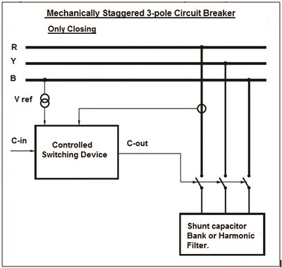
Figure 8: Schematic diagram of Machanically staggered 3-pole Circuit breaker (closing only)
Phases as per cofiguration in the Bus Circuit breaker Poles Staggering of closing instant, Eletrical degrees.
Care should be taken to connect the circuit breaker poles such that R-ph,S-ph & T- ph (or R,Y& B phases as per Indian convention) of the bus-voltage should be connected to C1,B1 A1 poles respectively of the circuit breaker.

Figure 9: Connection of Breaker poles to the Bus as per phase-wise configuration

Figure 10: The effect of staggering of breaker poles w.r.t.bus voltage-wave with referene to table no.1, above.
It is observed from the fig.10,
- when the S-ph voltage wave passes through ‘0’, at this instant, B1 pole of the Circuit breaker contacts make.
• At this instant the R –ph voltage wave shall be lagging behind by 240° ele and T – ph Voltage wave shall be lagging behind by 120° el to the S-ph voltage wave.
• Thus the R-Ph voltage wave shall cross the point”0” position at 60° ele while traversing from –ve to +ve cycle.
• The T-ph voltage wave shall cross the point “0” position at 120° ele. while travesing from +ve to –ve cycle.
• Had the poles of C1 & A1, not stagerred and adjusted, the voltage waves of R ph would have crossed the ‘0’ crossing after *3.33 ms and the T-Ph voltage wave would have crossed the ‘0’ crossing after after *6.66 ms as per prevailing system frequency of 50 Hzs in INDIA.
• Since the Stagerring of the Breaker poles is done resulting into closing all the 3-Ph contacts of the circuit breaker at the same instant.ie at voltage ‘0’ position for all the 3 Phases.
Note:
1) The constraint of connecting the Circuit breaker poles to individual phase as tabulated in the Table .No1 is essentiasl in case of grounded Shunt capacitor banks.
2) In case of un-grounded shunt capacitor banks such constraint is not there.
3) It is recommended that for Shunt Capacitor bank applications, 3-Pole operated Circuit breakers should be preferably used.
*Calculations to arrive at 3.33 ms and 6.66 ms.
Since 360o ele = 1 cycle = 20 ms,(since 50 cycles in 1 sec ie in 1000 ms).
∴ 60° ele ——– [(20 x 60)/360] = 3.33 ms. &
∴ 120° ele ————— 3.33 x 2 = 6.66 ms.
Essential Conditions For Successful Operations
- The System is programmed in such a manner that the closing command to the individual poles of the Circuit breaker is targetted to make the contacts of the poles at voltage ‘0’.The Closing command to individual closing coils of the individual poles is given accordingly as per difference of electrical degrees between them, by the Controlled switching Device (IED).
• Thus,it is essential that all the three poles of the Circuit breaker should have individual operating features (Closing & Opening).
• This system to function satisfactorily, it is essential that the accuracy limit at the instant of ‘0’ crossing of the system voltage (phase-wise) and the making of individual Circuit breaker poles should have an accuracy limit of ±1ms (approx.).
• The Circuit breaker should have rapid RDDS (Rate of Decrease Dielectric Strengh) ie on closing operation, the dielectric strength of the Circuit Breaker should rapidly decrease from high starting value to zero value.
• This system has an inter-lock for preventing the switching close-command to pass to the closing coil for 10 minutes.This feature takes care for the dis-charging time of the Capacitor banks.
A case-study of 2×33 MVAR, 145kV, Shunt Capacitor Banks at a 220kV S/S Gwalior in M.P. w.r.t. installation of 145kV SF6 Circuit breakers with Controlled Switching Device for each 33 MVAR Shunt capacitor bank.
2×33 MVAR, 145kV, Shunt Capacitor Banks were connected on to 132kV bus at 220kV S/S Gwalior in M.P.
Please refer to the following figures;
1) Fig: 11.. – Single line diagram of 2x33MVAR Capacitor bank with 1No. 145kV, SF 6 Circuit Breaker.
2) Fig 12.- Connection of 2×33 MVAR,145kV, Shunt Capacitor Bank on to the 132kV bus at 220kV S/S Gwalior in M.P.).
3) The 2×33 MVAR 145kV Capacitor banks are un-grounded banks having double star configuration.

Figure 11: Single line diagram showing 2×33 MVAR, 145kV.Shunt Cap. Banks, Controlled by 1- No. 145kV, SF6 CB only

Figure 12: S.L.D of 220kV & 132kV buses at 220kV S/s Gwalior under study in M.P.
The scenario has since been changed over a period of say 6 to 8 years due to the addition of 400kV and 765kV long Transmission lines (long and lightly loaded EHV Transmission lines generate Reactive Power) in the WREB Grid, now, only 1No-33 MVAR Shunt Capacitor bank is taken into service as and when required in this 220kV S/s Gwalior, under- study.
To highlight the benefits of taking the 33 MVAR Shunt capacitor bank into service, the readings taken on dated 27.11.2013 (reference: the S/S control room log-sheets) have been considered. The curves showing improvement in the voltage profile of 132kV bus, 220 kV bus and the MVAR injected by 1 No-33 MVAR, 145kV, Shunt capacitor Bank and its effect in terms of MVAR support on 132kV bus have been shown in the fig.13.

Figure 13: Curves pertain to the date: 27.11.2013 at the 220kV S/s Mahalgaon M.P. under study
Note: (refer fig.13).
Curves from top to bottom are designated serially in numerical order and are as follows;
- Curve No.1: 220kV bus voltage.
• Curve No.2: 132kV Bus voltage.
• Curve No.3 (red): Reactive loading in MVAR, on the 220/132kV Transformers on 132kV Bus.
• Curve No.4 (black): Injection of Reactive MVAR generated (MVAR Support) by 1x 33MVAR 145kV shunt Capacitor bank.
• As per convention, Reactive Support from Capacitor bank has been taken as (–) negative and Reactive loading (inductive) has been taken as (+) positive
As could be seen from the curve No.3 (red) that, though reactive compensation (capacitive) was being injected into the System, from 08.00 hrs to 14.00 hrs with a resultant of (–) 2 MVAR (Capacitive) at 132kV bus, suddenly Reactive MVAR loading increased to 12 MVAR (inductive) between 14.00Hrs to15.00 Hrs and thereafter the inductive/reactive loading further rose to 25 MVAR (inductive).
The curves shown in fig.13 have been judiciously drawn (on the basis of actual meter readings taken from the control room log-sheet) and looking to the same, another Switched 33 MVAR Shunt Capacitor bank should have been connected on to the 132kV Bus at 15.00hrs on 27.11.2013. However, the same could not be exercised, as out of the 2 Nos of 33 MVAR capacitor banks, only 1 No. Capacitor Bank was in service (The other 1No.Capacitor bank was kept out of service by isolating the same through a manually operated 145kV Isolating Switch).
To overcome such situations, an additional 145kV SF6 Circuit breaker (ND type) should be installed exclusively for controlling the 2nd-33 MVAR Shunt Capacitor Bank. The proposed Circuit Breaker’s control circuit should be equipped with Controlled Switching Device for eliminating the hazards of the transient inrush currents and the transient over voltages, which otherwise would have generated, as such a switching is categorized as Back to back Switching of Capacitor banks.
Conclusion
As could be seen from the above case-study, the M P Power Transmission Co Ltd should consider to install separate 145kV, SF6 Circuit breakers {ND-Type (Normal duty type)} with Controlled Switching Device, on the 2nd, 33 MVAR 145 kV Shunt Capacitor banks at the strategic 220kV S/Ss for switching-in onto the132 kV bus as and when the system demands (as back to bank switching).
Since the 145 kV, SF6 Circuit breakers are suitable for Capacitor Bank opening/tripping applications by way of having Re-strike free characteristics, the facility for tripping on faults /opening of Circuit breakers through Controlled switching Device is not essential. The other State Transmission Utilities and also the Govt. & Private entrepreneurs should follow the suit, wherever required.

If you want to share thoughts or feedback then please leave a comment below.


This is a valuable insight into how transient-free switching enhances the reliability and lifespan of switchgears. The focus on minimizing voltage spikes and ensuring smoother power transitions clearly highlights its role in protecting sensitive equipment, reducing maintenance needs, and improving overall system safety and efficiency.